
November - 2006 - issue > Company Profile
Applying Thought
Vidya Balakrishnan
Thursday, November 2, 2006

Applied Materials is changing all that. It is the global leader in nanomanufacturing technology solutions for the electronics industry.
It makes big, expensive machines that create tiny, precious microchips. “We are in every semiconductor [fabrication plant] and every flat panel fab in the world,” said Michael Splinter, CEO of Applied Materials.
The semiconductor equipment industry is a roughly $30 billion market; he estimates that related services constitutes about $11 billion, while the market for equipment for making flat-panel monitors and TVs is another $5 billion. Applied, which is expected to record $8.7 billion in revenues for its 2006 fiscal year ending in October, has a chance to gain market share, thanks to increasing demand for flat-panel displays and new trends such as multi-core processors. Applied Materials’ customers include chip makers such as Intel, Samsung and Texas Instruments, as well as companies who make semiconductor integrated circuits and manufacture the flat-panel displays used in monitors and TVs.
Chips are going to get more complex as we see more functions added to microprocessors. And with the industry moving towards systems-on-a-chip, it is critical for Applied Materials to adapt to the changing landscape. Advances in chip technology - including the shift from aluminum to copper, trimming of feature sizes to nanometer sub-micron levels and the move to 300-millimeter wafers – mean that in order to remain the envy of the equipment universe, Applied Materials must continue to extend its technical advantages while maintaining its close relationships with the chip manufacturers.
Manufacturing nanoscale chips encompasses hundreds of processes and each of these is implemented by complex equipment, sometimes as large as the device that they are being used to create. A single flat panel processing machine is shipped on Boeing 747 jet!
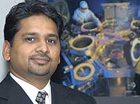
“We need to provide equipment that can increase the number of layers on a chip as well as get the layers tighter,” says Naren Dubey, Director of Global Development Capability (India, Russia and China). He returned to India last year to head Applied Materials India Development Center. Here, over 900 engineers participate in the product development, design, support and service functions for all of Applied Material’s product business groups.
Innovation does not stop with product development alone at Applied Materials. Amidst all the focus on technology, the center has not forgotten its roots in engineering services. Machines get redesigned and restructured very frequently to meet the dynamic nature of technology and this is where the service engineers at Applied Materials step in. Called the ‘process innovation’ or the Engineering Change Order, the service engineers work with the latest Six Sigma technology to analyze these changes and processes and then automate and improve them using the six-sigma productivity tools.
Use of six-sigma is fairly rampant in the industry and Applied Materials in India is using the six-sigma Methodology to quantify error rate and to improve the various processes across the organization verticals, thereby improving delivery and cycle time.
With the help of the six-sigma technology, the engineers at Applied Materials use the automation tools to reconfigure the process and then evaluate these designs. The six-sigma process quantifies error weights at every step and then provides the engineers with the next step to improve. The company then launches programs to improve every one of those steps.
The company had to step away from the local mindset to make use of the six-sigma technology. The results were for all to see. Using the six-sigma approach helped the engineers cut down 30 percent in error weights.
Though six-sigma is a relatively new approach as the tools were not available in India, the company moved away from the usual confined method of operating and into a global development functioning across the company. “It’s a mathematically rigorous approach, “ says Dubey, “And we are stretching the limits to the fullest.”
The Talent
For Dubey the real challenge has been in finding “People with background in designing complex menchano-electrical systems.” At the senior levels, Dubey looks for talent from automotive component design firms and power design companies. He has also been constantly looking for returnees—infusing experienced talent from the U.S. At the junior levels, hiring new graduates from top engineering schools is working pretty well.
Recently, during a company presentation at one of the IITs, Dubey asked a class of mechanical engineering students, “How many of you already have job offers from software firms?” Dubey wasn’t surprised to see 80 percent of the hands shoot up.
“Talented mechanical engineers are lured into software industry with high compensation. There is lack of awareness that companies like ours provide better opportunities to utilize their skills,” says Dubey. He has been touring several engineering colleges to change that perception. Even software engineers are welcome, provided their heart lay in engineering and material science interests them.
At Applied Materials India, there is an engineering governance board, which comprises engineering managers from multiple product groups. The board prepares the roadmap for the Bangalore Center in consultation with the company’s headquarters. The board also ensures that the engineers at the Bangalore center are involved in challenging tasks.
The engineers focus on innovating new concepts to reduce the cost of manufacturing electronic devices. “All of our engineers are given intellectually challenging assignments,” says Dubey.
“The kind of problems they have to tackle on a daily basis ensures that innovation forms the bedrock of all development activities here. We expose our engineers to complex engineering problems that have high cost pressure and short term delivery milestones. As long as they are faced with these challenges, innovation thrives in this atmosphere.” Creating newer versions, overcoming pitfalls, battling with market scenarios and designing a viable product—are all opportunities for innovating solutions. For example, a flat panel monitor used to cost $40,000 per piece because of the size of glass substrates on which transistors were made was less than a meter. Now through state-of-the-art process, the equipment can handle larger size substrates that lead to mass production of the substrates and contribute to their reduced cost.
With shortage of engineering design talent, Applied Materials wants to leverage best out of their employees. Hence it actively encourages cross-pollination of talent within. The best engineers from across different product groups are pooled in and share their ideas with each other. For example, say there are two product business groups that use plasma for different purposes; the first group for depositing material while the second group to etch or remove material. “We create a platform for both the groups to interact with each other and understand the behavior of plasma in different situations (depositing/etching). This throws up new ideas which may help in refining the processes they have been using,” says Dubey.
Engineers also have access to the top scientists within the company worldwide. Apart from their designated mentors, they can tap into functional domain experts. For example, anything related to fluid dynamics or radio frequency would be addressed by an identified subject expert.
Pravin Narwankar, CTO, Applied Materials India has visibility into the key technological areas that the company will likely set the agenda for advancement in the forthcoming years. He picks up few research areas and collaborates with academic institutes and sponsors research projects to translate those ideas into applied research. The India Center already has a tie-up with IIT Bombay and Indian Institute of Science, Bangalore. “Such an active engagement with the academic community would certainly quicken the progress in our R&D efforts,” says Narwankar. “We hope to engage these researchers in evolving nanomanufacturing processes for emerging technologies like carbon nanotubes, which is looked upon as the future technology.”
For now, everyone at the India Center seems excited. The India Development Center, like the other centers in China, Russia, Israel and U.K., coordinates with the headquarters in Santa Clara, which is the primary hub for all product development. The air is charged up with activity. Innovation thrives in the atmosphere!
 Cover Story")
 Cover Story")
 Cover Story")
 Cover Story")
 Cover Story")
 Cover Story")
 Cover Story")
 Cover Story")
 Cover Story")
 Cover Story")