The Futuristic View of Semiconductors

Technology as the disruptor has overhauled significant industries globally, and it has been the same with semiconductors too, facing 2X evolution every 18 months.
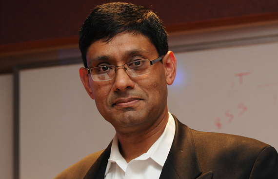
An industry veteran and technology leader Prith Banerjee, Chief Technology Officer at Ansys is effectively leading the advancing semiconductors industry, redefining strategy across the technology evolutions through simulation-based product innovation. Before joining Ansys, he has been in significant leadership roles across companies industry-wide. He spent the first 20 years in academia, as a professor at the University of Illinois and Northwestern University. Then he also held the Director’s role at HP Labs worldwide. He was also the CTO at two large industrial companies, ABB and Schneider Electric. In the CTO’s role at Ansys he is involved with setting the long-term technology strategy for the company through modelling and simulation working around areas such as high-performance computing, cloud, digital twins, use of AI, machine learning, and new areas such as healthcare and sustainability. He had recently been at the VLSI design conference where he presented a keynote talk on 'The future of simulation-based product innovation in the semiconductor industry'.
In a recent conversation with the Editor of Silicon India, Prith Banerjee, Chief Technology Officer at Ansys, shared his insights on the impact brought down by technology & emerging trends that would improve the efficiency of the semiconductors sector.
Semiconductor chips have rapidly evolved in the past few decades in terms of both speed and portability, can this growth keep on happening?
Looking at the consistent technology shifts around the industries, the disruption in semiconductors has been overwhelming and feels challenging. However, working according to Moore's law, in the last 30 years the industry has somehow been able to keep up with the dynamic challenges increasing the complexity of chips by a factor of 2 every 18 months. Where it was nearly impossible to overcome some of the fundamental challenges that emerged with the adding-up of numerous transistors on a single chip, today to complement it there’s the prowess of chiplets that can yield much higher results using 3D-IC technology. Each chiplet can either be the processor, the memory, GPU memory, or some sort of network processor. These are some of the technologies implying which the semiconductor industry is packing more and more technology on several transistors. So, we can have 100 billion transistors today in chips and we have great simulation technologies to support 3D-IC design, 2.5D, & 3D-IC designs and push forth these kinds of innovations.
What are the hurdles and risks faced in mass-producing semiconductor chips?
Now as things are getting more advanced, hurdles exist with the nodes. Earlier where the smallest of dimensions of chips used to be around 10 microns or 20 microns, now chips’ dimensions are extremely small, coming in sizes like two or three nanometres. It's very complicated to do such kinds of photolithography, and the challenges are faced with how to make photolithography work at two nanometres. Conclusively, semiconductor equipment companies like Applied Semiconductors, Lam Research, KLA Corporation, and others are extensively building on the latest technologies namely EUV. Engineering Simulation software companies such as Ansys are working with semiconductor equipment companies to ensure that the equipment will manufacture these small-size chips through simulation and further validation at the foundries such as TSMC/UMC/Global Foundries/Samsung & Intel. These foundries are used by fabless semiconductor companies like AMD, Broadcomm and Qualcomm. We at Ansys work with the entire ecosystem (equipment companies, foundries and fabless semi companies) to help drive the mass production of these chips and help lower the risks of manufacturing using simulation.
How has the manufacturing industry kept pace with the evolution of semiconductor chips?
Today’s semiconductor industry is evolving well through the right technology usage and proper simulation in semiconductors. In the past, where the 10-micron technology chips were manufactured using photoresistor technology and doing photolithography with masks on, including different other semiconductor manufacturing to do etching and so on, now it has become obsolete. As we shift to two nanometres’ size, some of the latest technologies like Chemical Vapour Deposition, Epitaxy, or EUV technologies prove to be extremely useful in performing fine-grain kinds of stuff. However, numerous challenges occur in the making of these complicated chips like tremendous signal integrity, thermal integrity, mechanical integrity, and others.
What is the future design of the modern chip? What is your opinion how would it go?
Transistors make up the basic fabric of a chip. Most of today’s chips contain billions of transistors, and some fantastic innovations are happening in chip manufacturing. The whole semiconductor industry has significantly evolved in the last 30 years, transitioning from the classic Horizontal/Planar transistors (P-type transistor, N-type transistor) to newer technologies like FinFET and Gate-All-Around (GAA) that function vertically to pack more transistors on a chip. However, as the transistor technology is evolving so are the simulation models keeping pace with the change.
Secondly, chip communication is also important. Say if there are one billion transistors on a chip and you have maybe 1000 pins on the chip, getting signals from outside the chip requires powering the IO pads of the chip which almost equals the power required by the computer. And, as the power required to drive the input-output signals is getting increasingly challenging, the whole industry has turned to optical interconnection. Thus using optoelectronic communication within the chips, light replaces electricity.
Furthermore, the third technology that this whole industry has got is Backside Power Delivery, which overrides the old, complicated chip planar technology and connects the power and the ground from the back of the chip. So essentially, the future semiconductor chip designer volunteers can use the technologies like gate-all-around Finfets, 3D-ICs, Optoelectronic communication, and backside power delivery to design the modern chips, which can be further validated and simulated by engineering simulation software.
What is the contribution of semiconductors to massive emerging trends such as cloud computing, 5G wireless network and Artificial Intelligence?
The semiconductor market is growing through leaps and bounds. Where it accounted for over $50 billion in 2021, the global semiconductor industry is anticipated to grow to $1 trillion in revenues by 2030, doubling in this decade. The factor leading to this growth is the increasing trend of companies towards Bespoke Silicon. Previously, it was only the semiconductor companies that used to build chips say, companies like Intel and AMD who were into manufacturing of processors; companies like Qualcomm and Broadcom, were making wireless chips, and the end users companies like Ford and GM (automotive industries), or Aerospace, or Defence companies used to source it. Now, each of the industries like the cloud is making its processors, their own interconnect chips to drive their data centres. For example, if Microsoft Azure is putting a cloud data centre, they are not getting their processors from Intel or AMD anymore, they are designing their own custom processors. Without a doubt, the whole semiconductor industry is going through Cloud, AI hardware, and more advanced technology. Now, in the era of Chatbots, AI, and GPT, which are quite complicated things implying to do training of 600 billion neurons and so on. Such large chips have to be built for different industries like Automotive, Aerospace, and Defence, including others, scope is abundant for semiconductors leveraging technologies such as AI, 5G/6G, Data centres, and Cloud computing to build.
In areas such as Advanced numerical methods, Advanced machines, AI Machine learning, High-performance computing, Digital twins and Cloud have much to offer. In my opinion, AI ML is one of the most important technology disruptors in this decade, and in the process to change and transferring simulations are lending a big hand to speed up fluid simulation by factors of 100. This will greatly improve and accelerate the way innovation is done, while completely automating the systems will improve the productivity of our scientists and engineers. Moreover, the other area is high-performance computing (HPC). The latest innovation that happened this year is a multi-GPU fluid solver that is going to run things like 30 to 100 times faster than what it could do. What this will enable all to do is help the automotive area or aerospace area customers to do a lot more accurate and a lot faster simulation. So, it will accelerate product innovation in the future, and establish India in the prolific chip supply chain and as a true world leader.
Read More News :
Integration of Technology in the Insurance Sector
How Software & Product Engineering is Furthering Business Resilience?


