 Magazine :
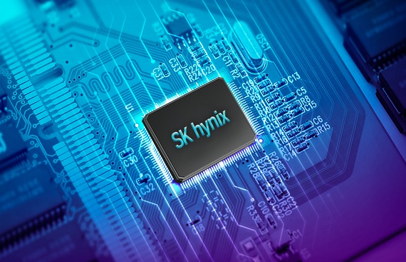
SK Hynix Evaluates Setting Up Memory Chip ATMP Facility In India
- SK Hynix enters exploratory talks with an Indian partner to set up a memory chip ATMP facility in India
- ASP Sealing Products confirms no diversification plans, while Odisha emerges as a frontrunner due to its revised semiconductor policy
- A potential SK Hynix investment is expected to boost India’s semiconductor ecosystem, especially in DRAM, NAND and advanced packaging
SK Hynix is in early talks with an Indian partner to jointly set up a memory chip ATMP facility in India. The discussions are still at the exploratory stage, and while the company reportedly reached out to Noida-based ASP Sealing Products to assess interest, ASP Sealing has clarified that it has no plans to diversify beyond its core automotive rubber components business. The two sides, therefore, are not currently pursuing an investment relationship.
In addition to its preliminary talks with private partners, SK Hynix has opened dialogue with multiple state governments to identify a suitable location for the proposed ATMP unit. Odisha has quickly emerged as a front-runner, driven by its revised semiconductor policy that offers aggressive financial and infrastructural incentives for chip-manufacturing projects.
India's national semiconductor mission is also playing a big role, having offered capital expenditure subsidies of up to 70 percent to global players willing to set up fabrication and packaging facilities in the country. Already, the incentive structure is showing momentum, with Micron Technologies building a $2.75 billion ATMP plant in Sanand, Gujarat, slated to produce more than 100 million units per month when fully functional.
A possible entry by SK Hynix will provide India's semiconductor ecosystem with the much-needed boost, notably in DRAM, NAND flash memory, and advanced packaging, where it is considered a world leader. The Tata Group's broader ambition within the space contributes further to the quickening pace of semiconductor expansion in India, driven by the planned high-volume chip facility that the company will establish in Assam, along with the -PSMC logic fab in Gujarat with a monthly capacity of 50,000 wafers.
Also Read: Fresh Week Fresh Moves as Tata IPO Buzz Sets the Market Abuzz
These are creating an evolving supply chain landscape marked by growing demand for cleanrooms, test and metrology equipment, high-density packaging substrates, automation solutions, and die-attach materials. Odisha's revised semiconductor policy looks arguably the most competitive in the country, offering early-stage support and better performance-linked incentives compared to previous versions.
The state has already received investments such as the silicon carbide fab of SiCSem and the advanced packaging unit of 3DGS, totaling investment commitments of more than Rs 4,000 crore. Potential locations for SK Hynix remain undecided but analysts list the Info Valley-II technology park in Bhubaneswar as one of the possible sites due to its infrastructure, connectivity, and logistics preparedness. But critical parameters include land allocation, uninterrupted power supply, long-term water planning, and availability of a technically trained workforce.
If SK Hynix eventually moves ahead with the project, it would further diversify India's semiconductor footprint and strengthen its emerging memory manufacturing ecosystem. The participation of the company would mean it would not only complement the existing logic fab developments but would add scale for domestic and global suppliers working across semiconductor testing, automation, and high-density system packaging.
Read More News :
Oracle India Marketing Head Geetu Bhatnagar Steps Down
TPG and Warburg Pincus Explore $500 Million Majority Stake in Sirion Labs