

C3Nano: Spearheading Innovations on the Touchscreen Front
The invention, mass market adoption, and popularity of touchscreens can be considered to be a turning point, a milestone, in the history of interfaces. Today, touchscreens are crucial components in reinventing a plethora of devices—that range from household appliances such as fridges, microwaves, TVs, and cameras to wearables such as watches, and even the good old projection screens—with the “smart” tag. That being said, smart devices manufacturers of all shapes and sizes, fueled by consumer demand and zeal to innovate, are constantly pushing the boundaries in terms of the technology and possibilities to make touchscreens more sleek, durable, and ergonomic: to make them more responsive, integrable to other functional components, transparent, conductive, thinner, bendable, stretchable, and ubiquitous.
The recent wave of foldable gadgets that hit the market, primarily smartphones, is a testament to this trend. To put in perspective, foldable screens hold the potential to redefine interfacing and inter activity while “widening the window” for newer applications and use scenarios. Helping some of the prominent and visionary enterprises in the smart devices realm, by innovating to eliminate the “touchscreen limitations” of their products at both manufacturing and prototyping levels, is California based C3Nano with their ActiveGrid™ and NanoGlueTM technologies.
C3Nano is the inventor and manufacturer of solution-based, transparent conductive films (TCF) and inks as direct replacements for traditionally preferred indium tin oxide (ITO). The latter has several performance barriers when it comes to achieving industry-leading conductivity and transparency in TCFs and inks. ITO is fundamentally a brittle materia precluding its use in flexible devices; it also has poor optical properties at low resitivities needed for large area touch. The cost of production of ITO is higher and it consequently impacts the cost of manufacturing touchscreen-enabled devices. The industry has long been on the lookout for viable alternatives for the multi-billion dollar display and consumer electronics industries.
C3Nano leverages cutting edge nanotech, and incorporates well-researched novelties at the material science and coating fronts to what in “touchscreen” language can be described as “effective in lowering sheet resistance to 30 ohms per square or less while maintaining excellent optical transparency and low haze.” Describing in layman terms, C3Nano draws chemically processed silver into nanowires that are a thousand times smaller in diameter than a strand of human hair. NanoGlueTM fuses the silver nanowires into conductive grids. C3Nano rolls out the technology as the product offering, ActiveGrid™ Film, which finds applications in smart windows, LCDs, E-paper, touch sensors, even solar cells and even some Bio-Tech applications. C3Nano’s technology engenders better optical performance than other ITO replacements, and has allowed for widespread adoption, serial production, and a plethora of commercial products incorporating C3Nano’s materials.
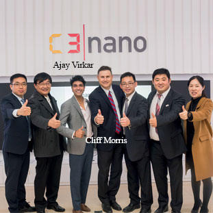
The company powers several new devices in the foldable gadgets space. They have also catered to the development and wide adoption of smart white boards and smart TVs, which serve the educational and business sectors in China, Europe and beyond. “For applications that intend to gain touch functionalities across large surface areas, one needs exceptionally good optical properties, and low resistivity, which our materials can easily achieve,” says Ajay Virkar, co-founder and CTO at C3Nano. “Although less visible to the general public, the growth of large area touch, is an exciting and huge market for materials companies like C3Nano; the forthcoming 5G network will also beget provacative new oppurtunities. In effect, the company delivers the enabling technology that makes electronics fundamentally flexible and robust.
Founded originally as a spinout from Stanford’s Zhenan Bao, C3Nano founding board member and Stanford University professor of chemical engineering— on carbon nanotubes, the company’s founders, back in 2010, were quick to notice the game-changing potential that touchscreens could have on both enterprise and consumer-spheres. They strategically re-purposed their mission to develop nanowire-based technology that is capable of producing flexible transparent conducting materials. Prominent venture capitalists were quick to grasp the unique value proposition of C3Nano, which has since successfully completed gainful rounds of funding and signed strategic partnerships. C3Nano’s investors and partners include GSR Ventures, Nissha Printing Co., Ltd., Phoenix Venture Partners, Hitachi Chemical, Lens Technology, Nagase America among others. Today, they have three facilities in California and China to manufacture their novel product stack. They also have sales and technical support across Asia.
Having carved a distinct niche for itself in the market, C3Nano continues to scale its operations while rigorously flexing its R&D muscles to drive more innovations into its offering. The company also plans to expand its partnership to be able to deliver solutions based on the custom requirements of its clients. “Our technology, outstanding team and partners, intellectual property, and focus on developing the best materials is what separates us from the rest of the players in the industry. The proliferation of touch sensors, flexible and non-planar electronics, and IoT and 5G revolutions all further fuel the widespread adoption and integration of our world-class materials,” concludes Virkar.C3Nano rolls out the technology as the product offering, ActiveGrid™ Inks and Films, which finds applications in smart windows, LCDs, E-paper, touch sensors, even solar cells and even Bio-Technology
